Get a quote

High-Frequency PCB

Electronic devices with high frequency are developing nowadays, especially in wireless networks. In addition, satellite communication is growing rapidly, and information products move towards high speed and high frequency.

What is high-frequency PCB?

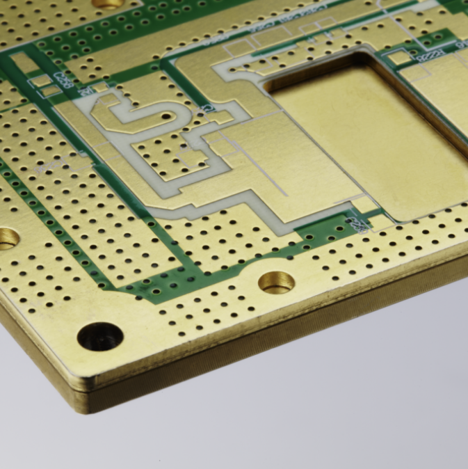
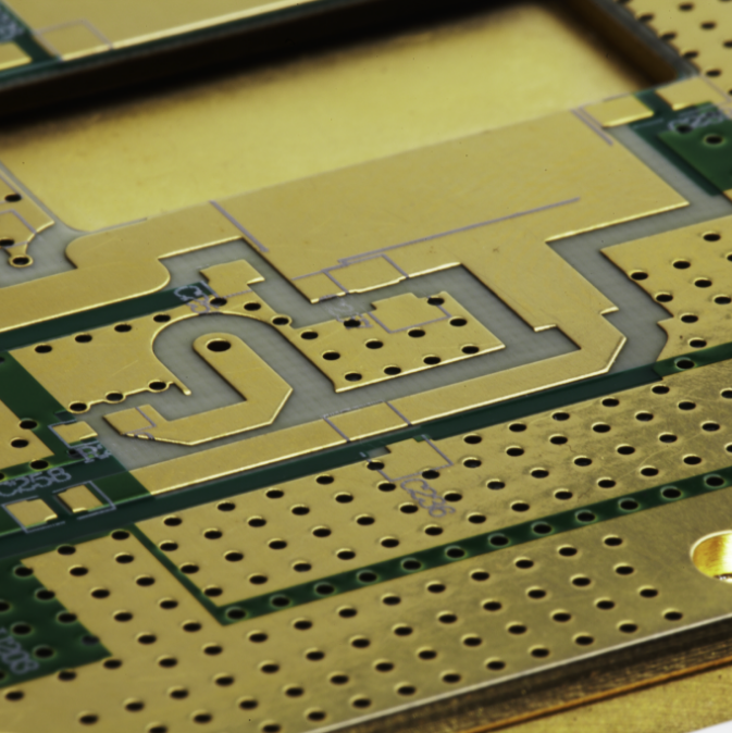
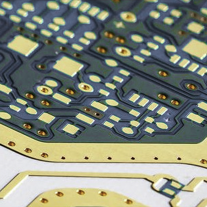
High-frequency PCBs are often needed while developing new high-frequency products, such as satellite systems, radio frequency, microwave, mobile telephone base stations, etc. These communication products usually use high-frequency substrates when designing the PCB.

It has a frequency range of 500MHz to 2GHz, perfect for high-speed designs. Higher transmission frequencies can also give faster signal flow rates, which are critical in today’s increasingly sophisticated electronic switches and other components.

How are high-frequency PCB boards made?

Certain materials are necessary to attain the high frequency afforded by this sort of printed circuit board; any changes in the Er value of these materials can impact the board’s impedance. Many PCB designers turn to Rogers, Taconic, and Arlon dielectric material due to its lower dielectric loss, less signal loss, lower circuit fabrication cost, and greater appropriateness for rapid prototyping applications.

Besides selecting the suitable PCB material and finding the correct Er value, designers need to consider parameters such as conductor width and spacing and the substrate constant. These parameters must be precisely determined and implemented with the tightest process control possible.

What materials are used for high-frequency PCBs?

When it comes to the cost of FR4, PPO, and Teflon laminates, FR4 is the least expensive, while Teflon is the most costly. Teflon is the best in terms of DK, DF, water absorption, and frequency characteristics. Only Teflon PCB substrate can be used to produce products that require frequencies more than 10GHz. Teflon’s performance is significantly superior to that of other substrates, yet, Teflon has the disadvantage of great heat resistance.

Capabilities

Feature

Capability

Material

Rogers, Arlon, Taconic, Neltec, etc.

Min. Track / Spacing

2 mil

Min. Hole Size

0.15 mm

Finished Cooper

1-2 oz

Board Thickness

0.2 - 3.2 mm

Surface Finishing

Immersion Gold, OSP, Hard Gold, Immersion Silver, Enepig

Finish Cooper

0.5-13 oz

Solder Mask

Green, Red, Yellow, Blue, White, Black, Purple, Matte Black, Matte Green

Silkscreen

White, Black

Via Process

Tenting Vias, Plugged Vias, Vias not covered

Testing

Fly Probe Testing (Free) and A.O.I. testing

Manufacturing time

7-10 days

Transport time

1-3 days

All you need to know about High Frequency PCB

High Frequency

A high frequency printed circuit board offers faster signal flow rates and a frequency range of up to 100 GHz. HF PCBs are defined by lower dielectric constant (Dk), lower dissipation factor (Df), and low levels of thermal expansion. They are used extensively in high speed communications, telecommunications, and RF microwave technology.

It depends on desired frequency, application and desired cost. Most common materials are ceramic filled hydrocarbon or PTFE. Key figures are low Dk and low dissipation factor.

Explore our other products

Standard PCB

Our definition of “Standard PCB” is a rigid glass-fibre board with one or more layers.

HDI PCB

High-dense-interconnect PCBs meet the demand for smaller PCB with more compact components by increasing wiring capabilities.

Flexible PCB

Flexible printed circuit boards get the name from the ability to be bent in a working application.

Rigid-Flex PCB

RIGID-FLEX PCB excels in overcoming space and weight constraints due to spatial degrees of freedom.

Metal Core PCB

A metal core printed circuit board uses metal as its base material to spread heat accumulated due to some electronic components operating on the board throughout the board.

Solder Paste Stencils

Customized high-precision laser-cut solder paste stencils are used by the subcontractor assembly company to apply solder paste with high accuracy to all places that shall be soldered.

Prototypes & Pilot Runs

PCB prototyping can be the most important step during electronic development.

Learn more how we ensure quality of our products.

Learn more

Capabilities

Feature Capability
Material Rogers, Arlon, Taconic, Neltec, etc.
Min. Track / Spacing 2 mil
Min. Hole Size 0.15 mm
Finished Cooper 1-2 oz
Board Thickness 0.2 - 3.2 mm
Surface Finishing Immersion Gold, OSP, Hard Gold, Immersion Silver, Enepig
Finsih Cooper 0.5-13oz
Solder Mask Green, Red, Yellow, Blue, White, Black, Purple, Matte Black, Matte Green
Silkscreen White, Black
Via Process Tenting Vias, Plugged Vias, Vias not covered
Testing Fly Probe Testing (Free) and A.O.I. testing
Manufacturing time 7-10 days
Transport time 1-3 days

Contact sales

Let’s get this conversation started. Tell us a bit about yourself, and your needs. We will get back to you within few hours.

Get a quotation

    We will get back to you within few hours