Get a quote

Printed Circuit Board - PCB

What is a PCB board?

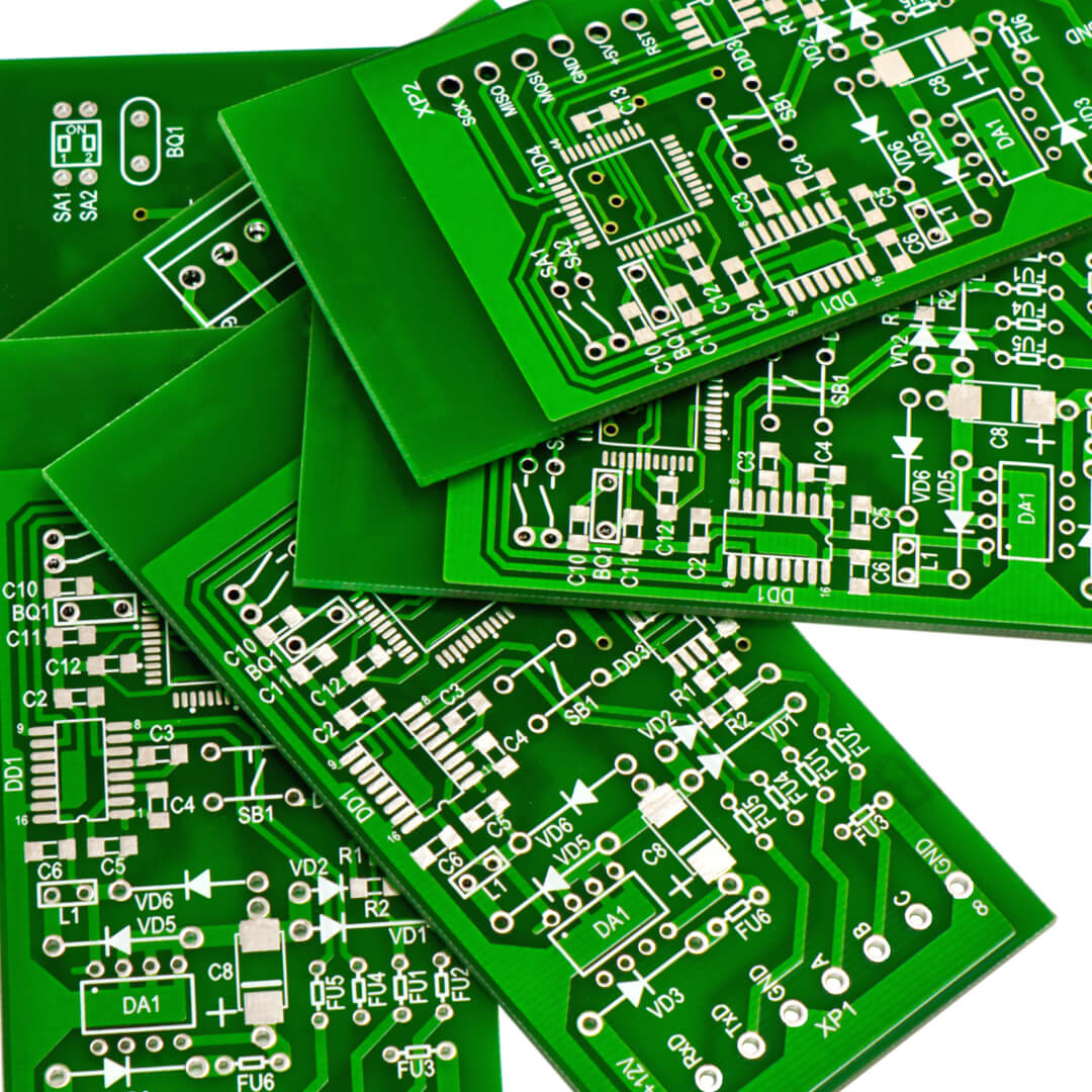
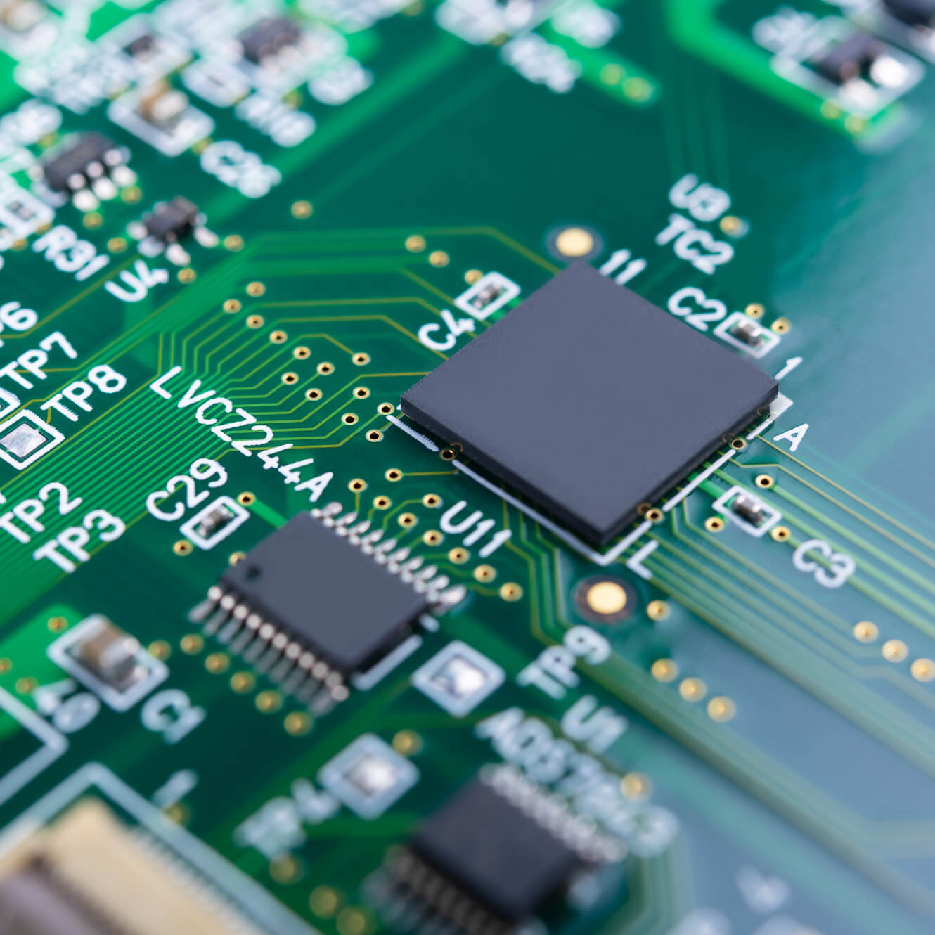
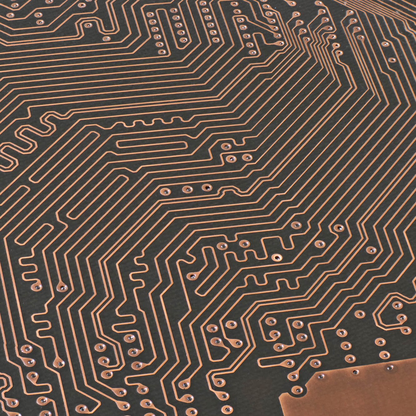
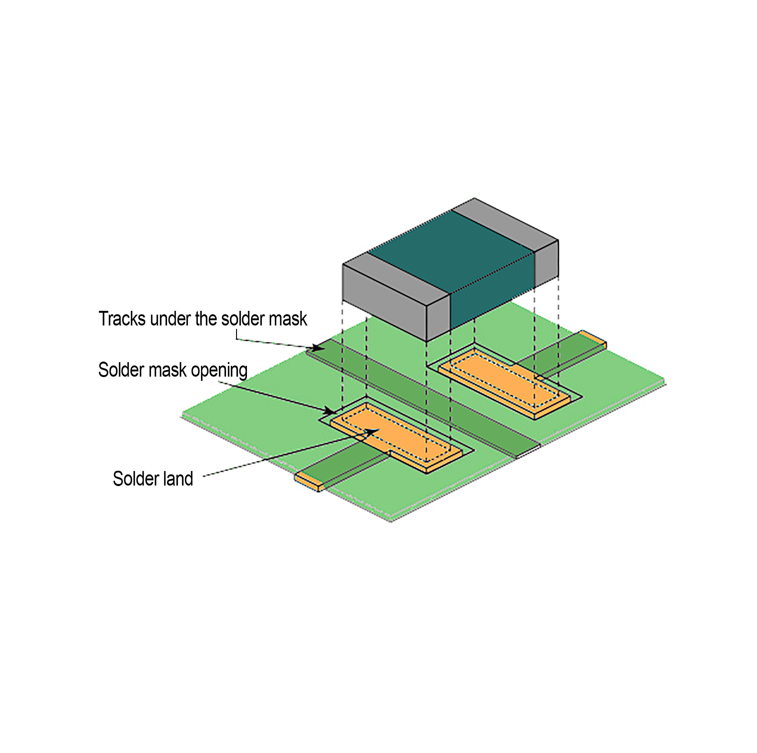
Printed circuit boards (PCBs) are the critical elements in the electronic devices since nearly 100 years. The PCB base is a non-conductive material with copper tracks printed and etched. Electronic components are mounted on the board, and the tracks connect the parts to form a working circuit.

What's a PCB?

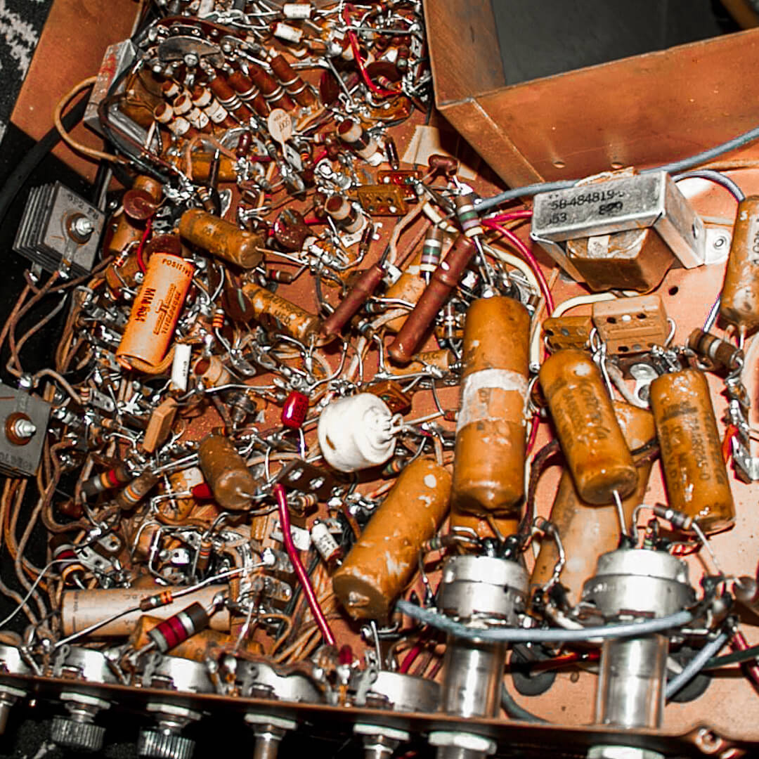
The printed circuit board is the most common name but may also be called “printed wiring boards” or just “the PCB”. Before the development of the PCB, circuits were constructed through a complicated process of point-to-point wiring. This led to frequent failures at wire junctions and short circuits when wire insulation began to age and crack.

A significant advance was the development of wire wrapping, where a small gauge wire is literally wrapped around a post at each connection point, creating a gas-tight connection which is highly durable and easily changeable. More about PCB history can be found in our blog section.

As electronics moved from vacuum tubes and relays to chip and integrated circuits, the size and cost of electronic components began to decrease. Electronics became more common in consumer goods, and the pressure to reduce electronic product size and production costs forced manufacturers to look for better solutions.

One of the key concepts in electronics is the printed circuit board or PCB. It’s so important that people often forget to explain what a PCB is. This page will try to explain what makes up a PCB and some of the common terms used in the PCB world.

Further down, we’ll discuss the build of a printed circuit board, link to some terminology.

Modern PCB

PCB is an acronym for the printed circuit board. It is a board with tracks and pads connecting various points together. In the picture above, some traces electrically connect the various components to each other. A PCB allows signals and power to be routed between physical devices. Solder is the metal that makes the electrical connections between the surface of the PCB and the electronic components. Being metal, solder also serves as a strong mechanical adhesive.

FR4

The base material, or substrate, is usually fiberglass and epoxy resin. Historically, the most common designator for this fiberglass is “FR4”. This solid core gives the PCB its rigidity and thickness. You will find many different thicknesses of PCBs, but the most common thickness for PCB is 1.6mm (0.063″), but a lot of different thicknesses are, of course, available.

Two-layer PCBs consist of an FR4 core and two layers of copper, but a “multi-layer” PCB can consist of several layers. The picture above shows a 4-layer PCB built with an FR4 core in center and carries layers 2 and 3. Outer layers (1 and 4) are built on FR4 prepreg that is pressed and hardened during the multi-layer pressing stage.

Besides the rigid FR4 base laminate, there is flexible PCB and also rigid-flex PCB, where the ability to bend the PCB or just some parts of the PCB board.

Copper

The conductive layer is a thin copper foil laminated to the board with heat and prepreg. On common, double-sided PCBs, copper is applied to both sides of the substrate. In lower-cost electronics, the PCB may have copper on only one side. When we refer to a double-sided or 2-layer board, we refer to the number of copper layers. This can be as few as 1 layer or as many as 16 layers or more.

The copper thickness can vary, but the standard is 35 um (0,035 mm). Some PCBs that handle very high power may use 70 or 105 um copper. Another way to define this is by the ounce (oz), where 1 oz is the same as 35 um.

Soldermask

The solder mask is the green cover on top of the copper foil. This mask gives the PCB its green appearance. It is overlaid onto the copper layer to insulate the copper traces from accidental contact with other metal, solder, or conductive bits. This cover helps the user to perform correct PCB soldering and prevent solder bridges.

In the example below, the green solder mask is applied to the majority of the PCB, covering up the small traces but leaving the solder lands and SMD pads exposed so they can be soldered.
Solder mask is most commonly green in colour but nearly any colour is possible.

Silkscreen

The white silkscreen print is applied on top of the solder mask layer. The silkscreen adds letters, numbers, and symbols to the PCB, allowing for easier assembly and indicators for humans to better understand the board. We often use silkscreen labels to indicate what the function of each pin or LED. PCB manufacturer often uses silk print to add their date and batch codes.

Silkscreen is most commonly white, but any ink colour can be used. Black, grey, red, and even yellow silkscreen colours are widely available; it is, however, uncommon to see more than one colour on a single board.

Where are PCB boards used?

It is used in most electronic products around us – smart watches, television, computers, or even electrical appliances like a washing machine or an iron – basically every modern item. While there are many different types of printed circuit boards, from one layer in cheaper consumer devices to more than 60 layers in advanced applications. All the PCBs play an important role in avoiding manual bailouts, automatic connection or soldering of electronic components, and testing as PCB consistency also has good quality for electronic devices, improves productivity.

PCBs can be divided into several different categories. From easy standard rigid boards to extreme designs with flexible- or other exotic materials. All depend upon what application the designer intends to create. Price can vary a lot between different solutions but is needed to get the desired performance.

Industries where PCBs are used

People use Printed Circuit boards in everyday life without even realizing it. Everything from personal goods such as smartphones and smartwatches to home appliances and entertainment systems such as televisions and video game consoles includes PCBs. But besides home and offices Printed Circuit board plays an essential part in a broad range of industries – automotive, medical, military, aerospace, construction, industrial, energy, data communication, and other sectors. In essence, the possibilities of using Printed circuit boards are endless. And as Printed Circuit boards evolve, they will find new applications in new industries.

Types of printed circuit boards

Standard PCB

Our definition of “Standard PCB” is a rigid glass-fibre board with one or more layers. This is by far the most common PCB in today’s production and will cover the most design needs.

HDI PCB

High-dense-interconnect PCBs meet the demand for smaller PCB with more compact components by increasing wiring capabilities. It makes the boards lighter, compact, and conserves space while maintaining excellent performance.

Flexible PCB

Flexible printed circuit boards get the name from the ability to be bent in a working application. This is called dynamic flex. Other flexible design is Intended to be folded to be able to fit a very narrow space in the final assembly.

Rigid-Flex PCB

RIGID-FLEX PCB excels in overcoming space and weight constraints due to spatial degrees of freedom. They can be used to benefit nearly all advanced electrical applications in medicine, military, aerospace, and consumer products, including testing equipment, tools, and automobiles. Apart from the Flexible PCB, the Rigid part of this design, can be made with the same design rules as a standard PCB, and increase the options for the final product.

Metal Core PCB

A metal core printed circuit board uses metal as its base material to spread heat accumulated due to some electronic components operating on the board throughout the board. It is widely used in LED technologies to enable high power in the industry of lighting.

High-Frequency PCB

High-frequency PCBs are often needed while developing high-frequency products, such as satellite systems, radio frequency, microwave, mobile telephone base stations, etc. These communication products usually use high-frequency substrates when designing the PCB.

Solder Paste Stencils

Customized high-precision laser-cut solder paste stencils are used by the subcontractor assembly company to apply solder paste with high accuracy to all places that shall be soldered. Fully optimized by our CAM engineers, we can assure seamless production; we support all known stencil-framing on the market.

Prototypes & Pilot Runs

PCB prototyping can be the most important step during electronic development. Not only for the designer to verify the function, but also to let the assembly unit check the effectiveness of production. MULTI-TEKNIK greatly reduces your costs and saves time when taking care of your prototype needs.

All you need to know about PCB´s

General

Yes. Since we have all kinds of factories, we can offer a wide range of delivery times. Also, many of our volume factories have prototype services in-house, so both prototype and volume will be produced in the factory.

Yes, there are still a lot of PCB manufacturers inside Europe, and we have carefully selected PCB manufacturers as our suppliers for express prototyping, but also a producer of solder paste stencils for PCB soldering. This laser-cut solder paste stencil can be of various types, such as vector guard, zellflex, genesis, and more, but also multi-level stencil.

All deliveries will pass Multi-Teknik quality control, and we check quality with the CAM-prepared data made at the beginning of the process. You will also have a CoC and quality control document along with the delivered PCB.

The straight answer is no. You will have the correct quantity of PCBs and only pay for the correct ones. The x-outs are not considered when counting and will not be included in the amount on the delivery note.

A PCB (printed circuit board) is a board with a printed copper pattern that forms a given circuit to enable the designer to connect several electronic components rationally. The most common material today for PCB boards is a combination of woven glass fiber and epoxy. For more demanding electronic designs, there are a lot of other base materials, such as ceramics, Teflon, polyimide, aluminum (mcpcb), and more.

The stack-up is the schematic view of how all copper layers, cores, and prepregs are grouped with data regarding thickness and material selections. Often impedance controlled PCB has this data in the stack-up view as well.

There is no exact date for the invention of the PCB; the truth is that it is a line of innovations that together contributed to today’s PCB. Of course, there is endless material about this on the Internet, but we have tried to pinpoint an unambiguous answer.

Mainly in China, where the world’s production is concentrated today, but also in Taiwan and inside Europe.

No one knows why just green became the standard color of PCB solder masks. But the rumor says that the electronic production staff in the USA during the second world war had voted about what colors were most friendly to eyes during a long time of work. And the green has become favorite.

Contact sales

Let’s get this conversation started. Tell us a bit about yourself, and your needs. We will get back to you within few hours.

Get a quotation

    We will get back to you within few hours